- 您现在的位置:买卖IC网 > Sheet目录323 > DSP56311EVM (Freescale Semiconductor)KIT EVALUATION FOR DSP56311
�� �
�
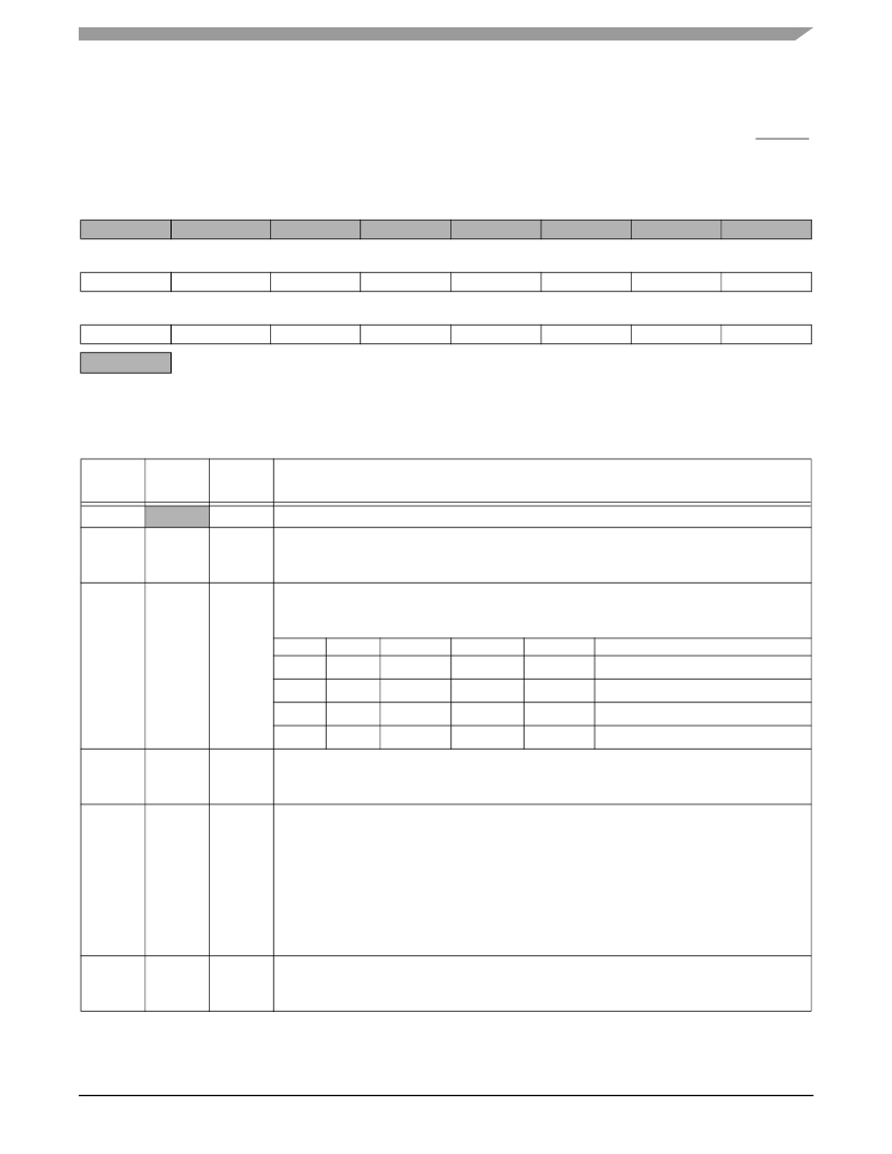
�SCI� Programming� Model�
�8.6.3� SCI� Clock� Control� Register� (SCCR)�
�The� SCCR� is� a� read/write� register� that� controls� the� selection� of� clock� modes� and� baud� rates� for�
�the� transmit� and� receive� sections� of� the� SCI� interface.� The� SCCR� is� cleared� by� a� hardware� RESET�
�signal.�
�23�
�15�
�TCM�
�7�
�CD7�
�22�
�14�
�RCM�
�6�
�CD6�
�21�
�13�
�SCP�
�5�
�CD5�
�20�
�12�
�COD�
�4�
�CD4�
�19�
�11�
�CD11�
�3�
�CD3�
�18�
�10�
�CD10�
�2�
�CD2�
�17�
�9�
�CD9�
�1�
�CD1�
�16�
�8�
�CD8�
�0�
�CD0�
�Reserved.� Read� as� 0.� Write� to� 0� for� future� compatibility.�
�Figure� 8-4.� SCI� Clock� Control� Register� (SCCR)�
�Table� 8-5.� SCI� Clock� Control� Register� (SCCR)� Bit� Definitions�
�Bit�
�Number�
�23–16�
�15�
�Bit� Name�
�TCM�
�Reset�
�Value�
�0�
�0�
�Description�
�Reserved.� Write� to� 0� for� future� compatibility.�
�Transmit� Clock� Source�
�Selects� whether� an� internal� or� external� clock� is� used� for� the� transmitter.� If� TCM� is� cleared,�
�the� internal� clock� is� used.� If� TCM� is� set,� the� external� clock� (from� the� SCLK� signal)� is� used.�
�14�
�RCM�
�0�
�Receive� Clock� Mode� Source�
�Selects� whether� an� internal� or� external� clock� is� used� for� the� receiver.� If� RCM� is� cleared,� the�
�internal� clock� is� used.� If� RCM� is� set,� the� external� clock� (from� the� SCLK� signal)� is� used.�
�TCM�
�0�
�0�
�1�
�1�
�RCM�
�0�
�1�
�0�
�1�
�TX� Clock�
�Internal�
�Internal�
�External�
�External�
�RX� Clock�
�Internal�
�External�
�Internal�
�External�
�SCLK�
�Output�
�Input�
�Input�
�Input�
�Mode�
�Synchronous/asynchronous�
�Asynchronous� only�
�Asynchronous� only�
�Synchronous/asynchronous�
�13�
�SCP�
�0�
�Clock� Prescaler�
�Selects� a� divide� by� 1� (SCP� is� cleared)� or� divide� by� 8� (SCP� is� set)� prescaler� for� the� clock�
�divider.� The� output� of� the� prescaler� is� further� divided� by� 2� to� form� the� SCI� clock.�
�12�
�COD�
�0�
�Clock� Out� Divider�
�output� is� a� 1� � clock.�
�Thus,� the� SCLK� output� is� a� 16� � baud� clock.�
�The� clock� output� divider� is� controlled� by� COD� and� the� SCI� mode.� If� the� SCI� mode� is�
�synchronous,� the� output� divider� is� fixed� at� divide� by� 2.� If� the� SCI� mode� is� asynchronous,�
�either:�
�?� If� COD� is� cleared� and� SCLK� is� an� output� (that� is,� TCM� and� RCM� are� both� cleared),� then�
�the� SCI� clock� is� divided� by� 16� before� being� output� to� the� SCLK� signal.� Thus,� the� SCLK�
�?� If� COD� is� set� and� SCLK� is� an� output,� the� SCI� clock� is� fed� directly� out� to� the� SCLK� signal.�
�11–0�
�CD[11–0]�
�0�
�Clock� Divider�
�Specifies� the� divide� ratio� of� the� prescale� divider� in� the� SCI� clock� generator.� A� divide� ratio�
�from� 1� to� 4096� (CD[11–0]� =� $000� to� $FFF)� can� be� selected.�
�DSP56311� User’s� Manual,� Rev.� 2�
�Freescale� Semiconductor�
�8-17�
�发布紧急采购,3分钟左右您将得到回复。
相关PDF资料
DSPAUDIOEVMMB1E
BOARD MOTHER DSP563XX
DSPIC30F2010 DEVELOPMENT KIT
KIT DEV EMBEDDED C
DSTRM-KT-0181A
DSTREAM DEBUG AND TRACE UNIT
DSUT1CSU
SURGE SUPPR NETWORK W/GROUND
DTEL2
SURGE SUPPRESSOR PHONE RJ11/RJ45
DV003001
PROGRAMMER PICSTART PLUS 16C/17C
DV164035
MPLAB ICD3 IN-CIRC DEBUGGER
DV164039
KIT DEV PIC24FJ256DA210
相关代理商/技术参数
DSP56311EVMIG_D
制造商:未知厂家 制造商全称:未知厂家 功能描述:DSP56311EVMIG DSP56311EVM Sample Code
DSP56311EVMUM
制造商:未知厂家 制造商全称:未知厂家 功能描述:DSP56311 Evaluation Module Hardware Reference Manual
DSP56311FACT
制造商:未知厂家 制造商全称:未知厂家 功能描述:DSP56311 Higher performance programmable DSP for demanding voice and data applications
DSP56311UM
制造商:未知厂家 制造商全称:未知厂家 功能描述:DSP56311 24-Bit Digital Signal Processor Users Manual
DSP56311UMAD
制造商:未知厂家 制造商全称:未知厂家 功能描述:DSP56311 Users Manual Addendum
DSP56311VF150
功能描述:数字信号处理器和控制器 - DSP, DSC 150Mhz/300MMACS 150Mhz EFCOP RoHS:否 制造商:Microchip Technology 核心:dsPIC 数据总线宽度:16 bit 程序存储器大小:16 KB 数据 RAM 大小:2 KB 最大时钟频率:40 MHz 可编程输入/输出端数量:35 定时器数量:3 设备每秒兆指令数:50 MIPs 工作电源电压:3.3 V 最大工作温度:+ 85 C 封装 / 箱体:TQFP-44 安装风格:SMD/SMT
DSP56311VF150B1
功能描述:数字信号处理器和控制器 - DSP, DSC 24 BIT DSP
RoHS:否 制造商:Microchip Technology 核心:dsPIC 数据总线宽度:16 bit 程序存储器大小:16 KB 数据 RAM 大小:2 KB 最大时钟频率:40 MHz 可编程输入/输出端数量:35 定时器数量:3 设备每秒兆指令数:50 MIPs 工作电源电压:3.3 V 最大工作温度:+ 85 C 封装 / 箱体:TQFP-44 安装风格:SMD/SMT
DSP56311VF150R2
功能描述:数字信号处理器和控制器 - DSP, DSC 24 BIT DSP RoHS:否 制造商:Microchip Technology 核心:dsPIC 数据总线宽度:16 bit 程序存储器大小:16 KB 数据 RAM 大小:2 KB 最大时钟频率:40 MHz 可编程输入/输出端数量:35 定时器数量:3 设备每秒兆指令数:50 MIPs 工作电源电压:3.3 V 最大工作温度:+ 85 C 封装 / 箱体:TQFP-44 安装风格:SMD/SMT